


The incredible PicoVNA: Low cost, high performance
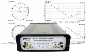
The PicoVNA 106 and PicoVNA 108 are low cost, small footprint, USB controlled Vector Network Analyzers that offer up to 8.5 GHz of bandwidth with performance that punches well above their weight.
Accurate: With up to 124 dB of dynamic range and RMS trace noise of just 0.005 dB at maximum resolution bandwidth, you know that what you are recording is a true reflection of the device you are measuring.
Fast: Capable of up to 5500 dual-port S-parameter measurements per second; that is, creating a 201-point two-port .s2p file takes less than 38 ms.
Affordable: Not only is the unit itself excellent value, calibration kits are highly affordable and easily repairable, keeping total cost of ownership low.
Reliable: The quad-RX architecture minimizes uncorrectable errors and delays.
Simple: Automated calibration with the E-Cal kit makes it easier and faster to get up and running.
 PicoVNA 5 software
The new PicoVNA 5 software makes measurements easy. The intuitive controls allow you to fully customize your viewports to your needs. Add a mix of frequency and time domain measurements, group markers across traces and configure readouts exactly how you need them.
Because PicoVNA is USB controlled, it is simple to save data to your drive — in a number of different formats including .csv and .s2p — to use with other software or share with your team.
For those who want to control their PicoVNA remotely, or perhaps want to run automated tests, the PicoSDK is also available with PicoVNAs. Control can be by either API calls or standard SCPI commands, and you can control multiple instruments at once.
The SDK works with Labview, MATLAB, Python and C/C++/C#. As you would expect, there are many examples to get you started on the Pico GitHub.

Simple, fast calibration
Calibrating your VNA can be a time-consuming and error-prone process, particularly for those new to microwave measurements. Using the automated Pico E-Cal can reduce errors and uncertainties, as well as increasing productivity by speeding up the calibration process, even while improving the quality of the resulting calibration.
Manual SOLT calibration kits are also available, with both male and female models and either standard (SMA) or premium (3.5 mm) connectors, and the Pico VNA 5 software will guide you through the whole process to minimize errors.

All Pico cal kits and check standards, whether automated or manual, are individually characterized using the more accurate TRL (through, line, reflect) calibration type. The kits are supplied with S-parameter data, allowing you to transfer the high quality characterization to your instrument as you calibrate it. This characterization process reduces the manufacturing cost of the cal kits without compromising on calibration quality; in fact, the correct port match is an excellent 46 dB typical on both source and load ports.
PicoVNAs support many calibration methods, including 8- and 12-term calibration, unknown through and also TRL and TRM (Through, Reflect, Line/Match). TRL and TRM calibrations are used when measuring a DUT mounted on a substrate, so are perfect for your network that’s already mounted to a PCB.

Customisable, board-only option for OEM
Many OEMs choose to integrate Pico hardware into their products. The board-only version of the PicoVNA 108 has a footprint of just 29 × 17 cm and all the same excellent specifications as the complete product.
Pico is the ideal choice for OEM applications and not just because of the excellent performance in a small footprint. Free technical support is available throughout the design process. The API provides complete control of the hardware, with code examples available on GitHub. Board- and FPGA-level modifications are also possible, making it possible to produce exactly the solution you need without compromises.
For more information and contact details, see our system integration hub.
Great for education

PicoVNAs have been designed with the professional user in mind, but that doesn’t mean they can’t be suitable for inexperienced hobbyists or students.
For educators, the Network Metrology Training Kit provides an ideal platform for covering all the basics of RF measurements. Included in the full kit is a PCB with a number of different circuits to test, plus a basic cal kit, N to SMA adaptors, SMA m-m and f-f adaptors, SMA test leads, a Pico wrench and a memory stick containing PicoVNA software (also available for download) and recommended software setups for use with the Kit.
Also included on the memory stick is comprehensive instructions demonstrating a huge variety of possible measurements, providing a great starting point for any RF training course or for self study.

The PCB itself has over ten different circuits. At one end of the board is a feed line based SOLT (short, open, load, through), for a different method of calibration. There is also a 25 Ω mismatched Beatty line, low pass and band pass Butterworth filters, an attenuator, a 6 dB power divider and space for adding your own 0603 component for testing. The final item on the board is a 6 GHz broadband amplifier (requires external +5 V DC supply, not supplied).
Paired with a PicoVNA, it provides an introduction to VNA measurements and high frequency design. Once the basics have been grasped, it also allows demonstration of more complex topics such as P1dB and AM to PM conversion.
To take it one step further, Pico has partnered with Cadence AWR Microwave Office. The PCB files for the Network Metrology Training Kit are available to import to Microwave Office so you can compare simulations and real-world measurements. Even better, Pico’s Cadence AWR DE Interface wizard allows you to import VNA measurements to enhance your simulation.
Get connected
Your PicoVNA comes bundled with everything to get the unit up and running: USB 2 cable, a power supply (12 V 3.5 A universal supply), two RF combination spanners and a sturdy carry case to keep it all in, plus a USB drive with the PicoVNA software and digital copies of the user guide. Measurement cables are available separately – see the accessories page for details.
‘Quad RX’ four-receiver architecture
In a VNA a swept sine-wave signal source is used to sequentially stimulate the ports of the interconnect or device under test. The amplitude and phase of the resultant transmitted and reflected signals appearing at both VNA ports are then received and measured. To wholly characterize a 2-port device under test (DUT), six pairs of measurements need to be made: the amplitude and phase of the signal that was emitted from both ports, and the amplitude and phase of the signal that was received at both ports for each source. In practice this can be achieved with a reasonable degree of accuracy with a single source, a transfer switch and two receivers; the latter inputs being switched through a further pair of transfer switches. Alternatively three receivers can be used with an additional input transfer switch or, as in the PicoVNA, four receivers can be used. Using four receivers eliminates the receiver input transfer switch errors (chiefly leakage and crosstalk) that cannot be corrected. These residual errors are always present in two- and three-receiver architectures and lead to lower accuracy than that of the Quad RX design.
Support for 8 and 12-term calibration and the unknown thru
Almost all vector network analyzers are calibrated for twelve error sources (six for each signal direction). This is the so-called 12-term calibration, which experienced VNA users are used to performing fairly regularly. In a four-receiver design some error sources are so reduced that 8-term calibration becomes possible, along with an important and efficient calibration technique known as the unknown thru. This gives the ability to use any thru interconnect (including the DUT) during the calibration process, vastly simplifying the procedure and reducing the number of costly calibration standards that need to be maintained.
Advanced vector network analyser users will be pleased to know that internal a-wave and b-wave data is made available for export under a diagnostic facility. Amongst others, Transfer switch error terms can therefore be derived.

Bias-Ts
Bias-Ts are often not provided, or available as costly extras, on other VNAs. Use the PicoVNA 106’s built-in bias-Ts to provide a DC bias or test stimulus to active devices without the complexity and cost of external DC-blocks. The bias is supplied from external power supplies or test sources routed to the SMB connectors adjacent to each VNA port.

Test cables and calibration standards
A range of RF and Microwave accessories are available from Pico Technology. Test cables and calibration standards have particular significance to the overall performance of a VNA, so we recommend that you select your accessories carefully. Cables and standards are often the weakest links in a VNA measurement, generally contributing significantly to measurement uncertainty despite their high cost. At the lowest levels of uncertainty, costs can be significant and measurements can be compromised by seemingly quite minor damage or wear. For these reasons, many customers hold both premium-grade items for calibration, reference or measurement standards, and standard-grade items as working or transfer standards and cables. Pico Technology can now offer cost-effective solutions in both grades.
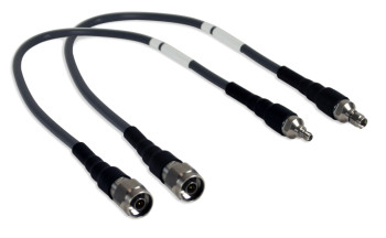
Phase- and amplitude-stable test leads
Two test cable types and grades are recommended and provided by Pico Technology. Both of high quality, with robust and flexible construction and stainless steel connectors, the main difference between them is the stability of their propagation velocity and loss characteristic when flexed; that is, the degree to which a measurement could change when the cables are moved or formed to a new position. Cables are specified in terms of flatness and phase variation at up to 6 GHz when a straight cable is formed as one 360° turn around a 10 cm mandrel.
Recommended Products
| Product | Price | Quantity | |
|---|---|---|---|
 |
Standard 8.5 GHz SOLT calibration kit (SMA male) TA344 Recommended |
||
 |
Standard 8.5 GHz SOLT calibration kit (SMA female) TA345 Recommended |
||
 |
Premium 8.5 GHz SOLT calibration kit (PC3.5 male) TA346 Recommended |
||
 |
Premium 8.5 GHz SOLT calibration kit (PC3.5 female) TA347 Recommended |
||
 |
Standard 8.5 GHz phase stable test lead, female port, N(m) – SMA(f) TA337 Recommended |
||
 |
Standard 8.5 GHz phase stable test lead, male port, N(m) – SMA(m) TA336 Recommended |
||
 |
Premium 8.5 GHz flex-form test lead, male port, N(m) – PC3.5(m) TA338 Recommended |
||
 |
Premium 8.5 GHz flex-form test lead, female port, N(m) – PC3.5(f) TA339 Recommended |
||
 |
Standard test port adaptor, SMA(m-m) TA342 Recommended |
||
 |
Standard test port adaptor SMA(f-f) TA343 Recommended |
||
|
Premium test port adaptor PC3.5(m-m) TA340 Recommended |
||
|
Premium test port adaptor PC3.5(f-f) TA341 Recommended |
||
 |
Calibration certificate and data for PicoVNA CC046 Recommended |
||
 |
Network Metrology Training kit and carry case PQ186 Recommended |
||
 |
Network Metrology Training printed circuit assembly and carry case PQ189 Recommended |
||
 |
Network Metrology Standard SMA(f) Demonstrator kit and carry case PQ187 Recommended |
||
|
Network Metrology Premium PC3.5(f) Demonstrator kit and carry case PQ188 Recommended |
||
 |
Dual-break torque wrench SMA / PC3.5 / K-type TA356 Recommended |
||
 |
Dual-break torque wrench N-type connector TA358 Recommended |
||
 |
SOLT-STD-M or SOLT-STD-F calibration data CC047 Recommended |
||
|
SOLT-PREM-M or SOLT-PREM-F calibration data CC048 Recommended |
||
 |
CHK-NON-F Noninsertable check standard SMA(f-f) TA431 Recommended |
||
 |
CHK-INS-MF Insertable check standard SMA(m-f) TA430 Recommended |
||
 |
Training SMA(f) SOLT Calibration Kit PQ190 Recommended |
||
 |
ADA-PREM-FM Premium within series adaptor PC3.5(f-m) TA354 Recommended |
||
 |
ADA-STD-FM Standard within series adaptor SMA(f-m) TA357 Recommended |
||
|
CHK-NON-F or CHK-INS-MF check-standard calibration CC050 Recommended |
||
 |
PicoVNA Dual E-Cal 8.5 GHz Automated calibration kit (SMA) TA520 Recommended |
||
 |
PicoVNA E-Cal 8.5 GHz Automated calibration kit (SMA female) TA519 Recommended |
||
 |
PicoVNA E-Cal 8.5 GHz Automated calibration kit (SMA male) TA518 Recommended |
||
 |
SOLT-AUTO-M or SOLT-AUTO-F calibration data CC057 Recommended |
||